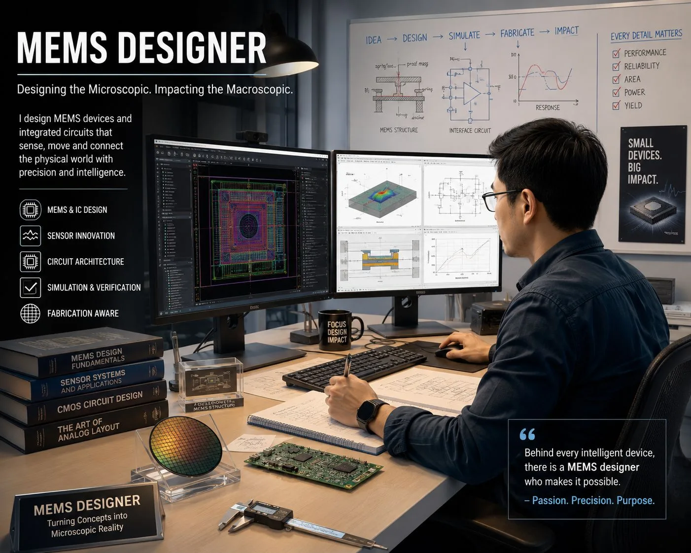
Looking at those project accounts today, I often ask a simple question:
What if today's AI had been part of those workflows back then?
I believe it could have reduced nearly 90% of the low-value repetitive work tied to those projects, while maintaining accuracy approaching 99.9999% for structured, rule-driven tasks. In financial terms, that translates into lower project burn rates, lebih pantas development cycles, and quicker capitalization of R&D assets.
Notice that I said repetitive workload, not engineering judgement.
IC development has never been just about circuit diagrams. Engineers spend large portions of their time searching documentation, checking design rules, generating reports, comparing revisions, validating parameters, and ensuring compliance with manufacturing constraints. From an accounting perspective, these are cost-bearing activities with predictable inputs-exactly the structured tasks where AI can deliver measurable return.
Fast forward to today.
The AI conversation has shifted from "Which model is the smartest?" to "How should AI be integrated so that it protects margins and improves project predictability?"
From a financial operations perspective, the future of semiconductor engineering is not about removing engineers from the payroll.
It is about reallocating expensive engineering capacity toward high-value problem-solving while AI handles repetitive, deterministic processes.
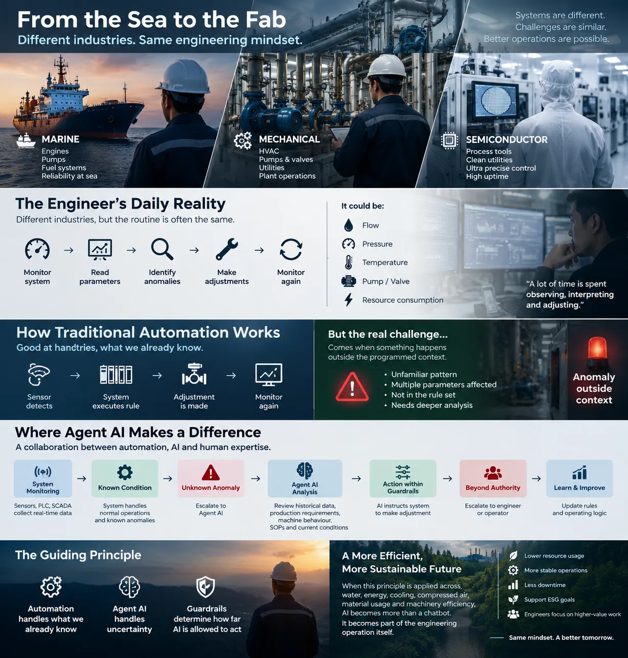
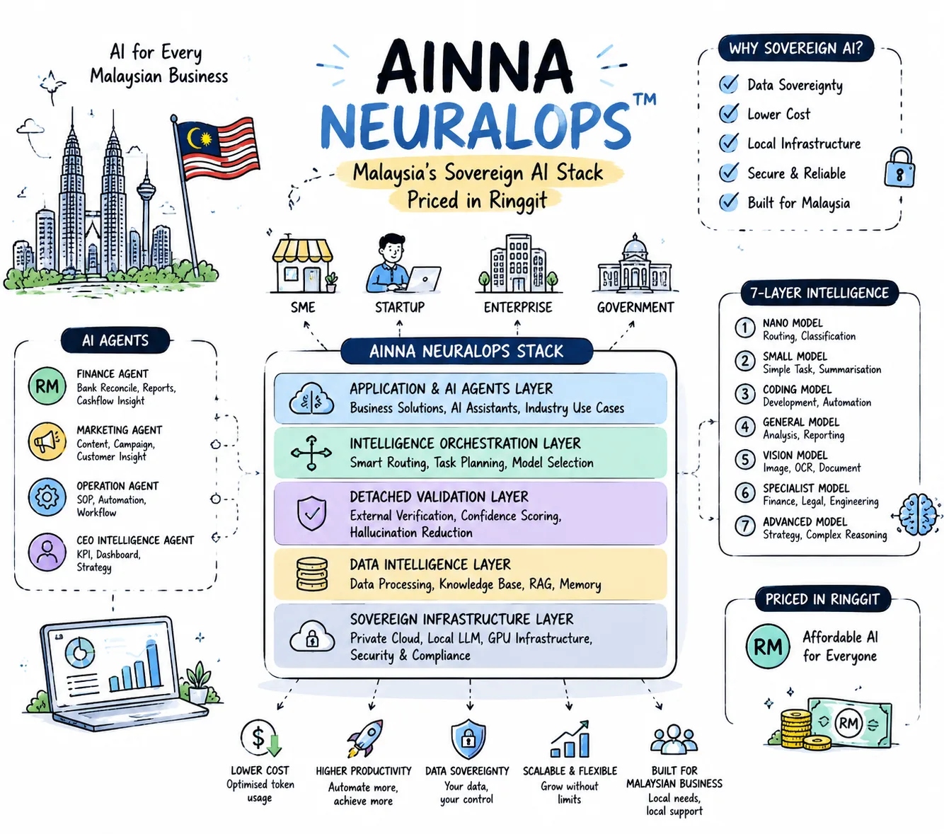
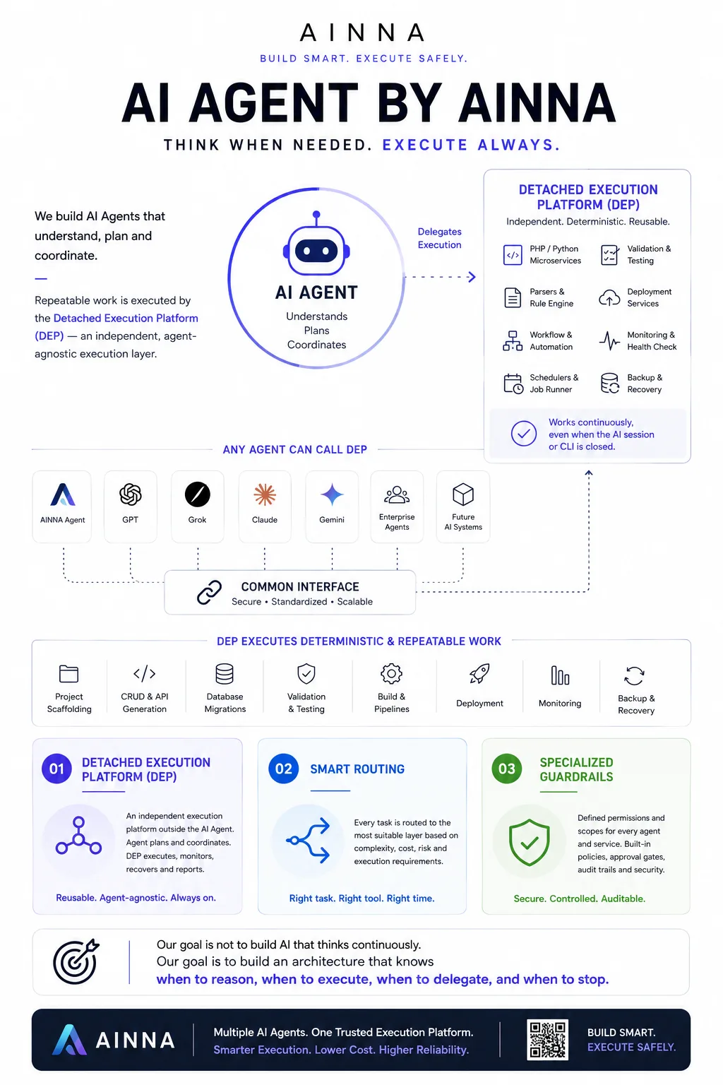
This is also why I pay close attention to AI infrastructure and architecture from an asset-management viewpoint. The objective is not simply to deploy the largest language model, but to build systems that know when AI should be used-and when traditional software, parsers, rules engines, or deterministic workflows are the more cost-effective choice.
In semiconductor design, every unnecessary verification cycle adds to project cost and delays revenue recognition.
Every design respin consumes budget, inventory, and working capital.
Every engineering hour saved shortens the path from concept to silicon and improves return on R&D investment.
That is why I view AI as an essential operational asset for IC and semiconductor teams. Its value is not headcount reduction; it is enabling engineers to focus on innovation instead of repetitive execution, while finance teams see improved cost control and project visibility.
Having reviewed engineering project finances before today's AI era, I appreciate how transformative this technology can be when applied with the right architecture and governance.
The next generation of IC design will not be powered by smarter AI alone.
It will be powered by smarter, more cost-efficient engineering workflows.
Official Cross-Rangkaian Resource













Ruang pembaca
Apa pendapat anda?
Komen baharu dihantar untuk semakan terlebih dahulu. Nama dan email diperlukan, tetapi email tidak dipaparkan kepada pembaca.
The numbers around every iteration consumes billable hours make more sense than most posts I read.
The bit about whether the work is MEMS is what I keep coming back to. Have a few questions left here.
rule-driven tasks - that is the whole thing in one line.
Sigo pensando en 90%.
Honestly deterministic processes.This caught me off guard.
Still thinking about checking design rules, generating reports.
maintaining accuracy approaching 99.9999% is what I would forward to my boss.
Clear and short. Sharing documentation updates with my team.
I would push back slightly on revised schedules, additional verification, but the direction is right. Still thinking this one through.
I read this twice. have reduced nearly 90% is the part that stuck.
Whoever wrote this actually did the work on IC layout, or system verification.
I have watched software licences, foundry fees go wrong in practice. Good to see it written down.
This is where every unnecessary verification cycle adds finally clicks.
The framing on lebih pantas development cycles is better than expected.
90% bagian yang mau saya kirim ke atasan.
Sent this to two people already. comparing revisions, validating parameters is why. Have a few questions left here.