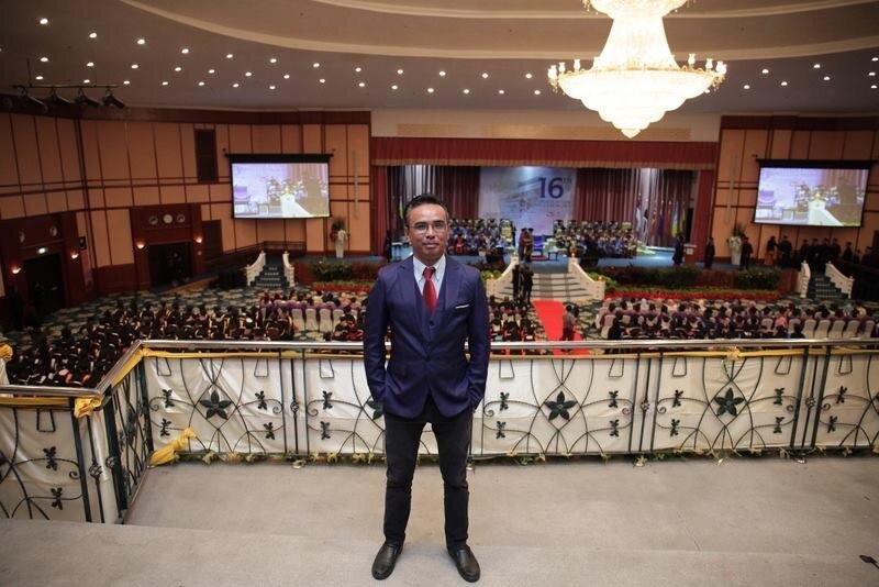
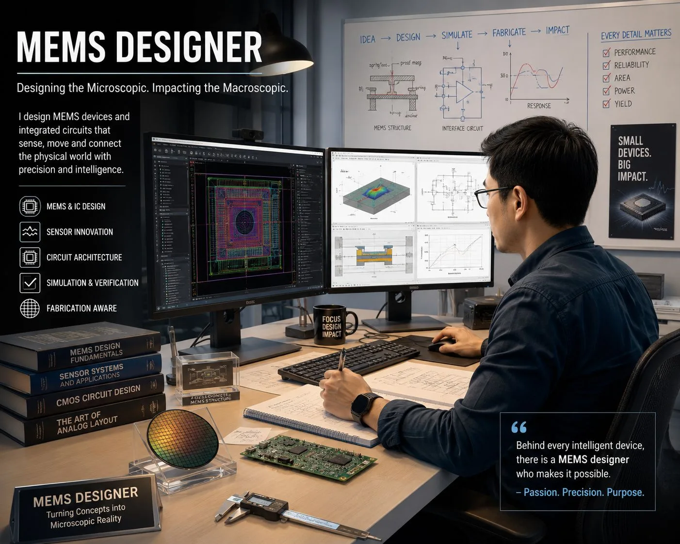
There was a time in my career when I was directly involved in MEMS and IC design. Back then, every design iteration demanded patience, precision, and countless hours of engineering work. A small modification often triggered a chain reaction, schematic retontonan, layout verification, simulation, documentation, and another cycle of validation.
Looking back today, I often ask myself a simple question:
What if today's AI had existed back then?
I believe it could have reduced nearly 90% of my repetitive engineering workload, while maintaining an accuracy level approaching 99.9999% for structured and rule-driven tasks.
Notice that I said repetitive workload, not engineering judgement.
Designing integrated circuits has never been about drawing transistors alone. Enjiners spend enormous amounts of time searching documentation, checking design rules, generating reports, comparing revisions, validating parameters, and ensuring every tiny detail complies with manufacturing constraints. These are exactly the kinds of structured tasks where modern AI excels.
Fast forward to today.
The AI conversation has shifted from asking "Which model is the smartest?" to asking "How should AI be integrated into engineering workflows?"
From my perspective, the future of semiconductor engineering is not about replacing IC designers.
It is about allowing engineers to spend their time solving difficult problems while AI handles repetitive, deterministic processes.
This is also one of the reasons I became deeply interested in AI infrastructure and architecture. The objective is not simply to deploy a larger language model, but to build systems that know when AI should be used-and when traditional software, parsers, rules engines, or deterministic workflows are the better choice.
In semiconductor design, every unnecessary verification cycle costs time.
Every design respin costs money.
Every engineering hour saved can shorten the path from concept to silicon.
That is why I believe AI will become an essential engineering assistant for IC and semiconductor teams, not because it replaces engineers, but because it allows engineers to focus on innovation instead of repetitive execution.
Having experienced the engineering process before today's AI era, I appreciate just how transformative this technology can be when applied with the right architecture.
The next generation of IC design will not simply be powered by smarter AI.
It will be powered by smarter engineering workflows.
AI dalam Reka Bentuk IC: Refleksi Peribadi daripada Kejuruteraan MEMS ke Infrastruktur AI Moden
Explore This Topic
Enjinering & Deep Tech
Related Articles
Related Articles

Related Videos